- 您现在的位置:买卖IC网 > Sheet目录1201 > CDB5461AU (Cirrus Logic Inc)BOARD EVAL & SOFTWARE CS5461A
�� �
�
�CS5461A�
�The� Cycle� Count� Register� (N)� must� be� set� to� a� value�
�greater� than� one.� Status� bit� TUP� in� the� Status� Register,�
�indicates� when� the� Temperature� Register� is� updated.�
�The� Temperature� Offset� Register� sets� the� zero-degree�
�measurement.� To� improve� temperature� measurement�
�accuracy,� the� zero-degree� offset� should� be� adjusted� af-�
�ter� the� CS5461A� is� initialized.� Temperature� offset� cali-�
�bration� is� achieved� by� adjusting� the� Temperature� Offset�
�Register� (T� off� )� by� the� differential� temperature� (� ?� T)� mea-�
�sured� from� a� calibrated� digital� thermometer� and� the�
�CS5461A� temperature� sensor.� A� one-degree� adjust-�
�ment� to� the� Temperature� Register� (T)� is� achieved� by�
�adding� 2.737649x10� -4� to� the� Temperature� Offset� Regis-�
�ter� (T� off� ).� Therefore,�
�A� hardware� reset� is� initiated� when� the� RESET� pin� is� as-�
�serted� with� a� minimum� pulse� width� of� 50� ns.� The�
�RESET� signal� is� asynchronous,� with� a� Schmitt-trigger�
�input.� Once� the� RESET� pin� is� de-asserted,� an�
�eight-XIN-clock-period� delay� is� enabled.�
�A� software� reset� is� initiated� by� writing� the� command� of�
�0x80.� After� a� hardware� or� software� reset,� the� internal�
�registers� (some� of� which� drive� output� pins)� will� be� reset�
�to� their� default� values.� Status� bit� DRDY� in� the� Status�
�Register,� indicates� the� CS5461A� is� in� its� active� state�
�and� ready� to� receive� commands.�
�5.10� Power-down� States�
�The� CS5461A� has� two� power-down� states,� stand-by�
�T� off� =� T� off�
�+� ?� ?� T� ?� 2.737649� ?� 10� –� 4� ?�
�and� sleep.� In� the� stand-by� state� all� circuitry� except� the�
�voltage� reference� and� crystal� oscillator� is� turned� off.� To�
�if� T� off� =� -0.0951126� and� ?� T� =� -2.0� (� o� C),� then�
�return� the� device� to� the� active� state� a� power-up� com-�
�mand� is� sent� to� the� device.�
�T� off� =� –� 0.0951126�
�+� ?� –� 2.0� ?� 2.737649� ?� 10� –� 4� ?�
�=� –� 0.09566�
�In� sleep� state� all� circuitry� except� the� instruction� decoder�
�is� turned� off.� When� the� power-up� command� is� sent� to�
�F� =� ---� ?� C� +� 17.7778� ?�
�or� 0xF3C168� (2’s� compliment� notation)� is� stored� in� the�
�Temperature� Offset� Register� (T� off� ).�
�To� convert� the� Temperature� Register� (T)� from� a� Celsius�
�scale� (� o� C)� to� a� Fahrenheit� scale� (� o� F)� utilize� the� formula�
�o� 9� o�
�5�
�Applying� the� above� relationship� to� the� CS5461A� tem-�
�perature� measurement� algorithm�
�the� device,� a� system� initialization� is� performed� (see�
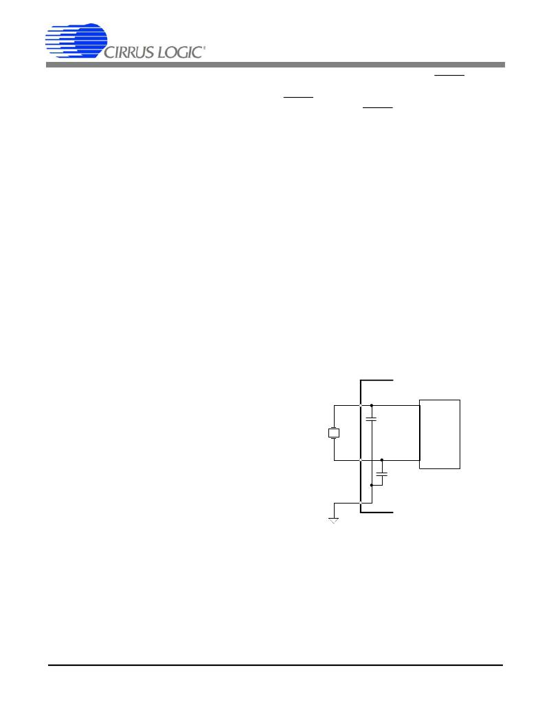
��5.11� Oscillator� Characteristics�
�The� XIN� and� XOUT� pins� are� the� input� and� output� of� an�
�inverting� amplifier� configured� as� an� on-chip� oscillator,�
�as� shown� in� Figure� 8.� The� oscillator� circuit� is� designed�
�XOUT�
�T� ?� F� ?� =�
�o�
�?� 9� --� 5� -� ?� T� gain� ?� ?� T� ?� o� C� ?� +� ?� T� off� +� ?� 17.7778� ?� 2.737649� ?� 10� –� 4� ?� ?� ?�
�C1�
�Oscillator�
�Circuit�
�If� T� off� =� -0.09566� and� T� gain� =� 23.507� for� a� Celsius�
�scale,� then� the� modified� values� are� T� off� =� -0.0907935�
�(0xF460E1)� and� T� gain� =� 42.3132� (0x54A05E)� for� a�
�Fahrenheit� scale.�
�XIN�
�C2�
�5.8� Voltage� Reference�
�The� CS5461A� is� specified� for� operation� with� a� +2.5� V�
�reference� between� the� VREFIN� and� AGND� pins.� To� uti-�
�DGND�
�C1� =� C2� =� 22� pF�
�lize� the� on-chip� 2.5� V� reference,� connect� the� VREFOUT�
�pin� to� the� VREFIN� pin� of� the� device.� The� VREFIN� pin�
�can� be� used� to� connect� external� filtering� and/or� refer-�
�ences.�
�5.9� System� Initialization�
�Upon� powering� up,� the� digital� circuitry� is� held� in� reset�
�until� the� analog� voltage� reaches� 4.0� V.� At� that� time,� an�
�eight-XIN-clock-period� delay� is� enabled� to� allow� the� os-�
�cillator� to� stabilize.� The� CS5461A� will� then� initialize.�
�20�
�Figure� 8.� Oscillator� Connection�
�to� work� with� a� quartz� crystal.� To� reduce� circuit� cost,� two�
�load� capacitors� C1� and� C2� are� integrated� in� the� device,�
�from� XIN� to� DGND,� and� XOUT� to� DGND.� PCB� trace�
�lengths� should� be� minimized� to� reduce� stray� capaci-�
�tance.� To� drive� the� device� from� an� external� clock�
�source,� XOUT� should� be� left� unconnected� while� XIN� is�
�driven� by� the� external� circuitry.� There� is� an� amplifier� be-�
�tween� XIN� and� the� digital� section� which� provides�
�CMOS-level� signals.� This� amplifier� works� with� sinusoi-�
�DS661F3�
�发布紧急采购,3分钟左右您将得到回复。
相关PDF资料
CDB5466U
BOARD EVAL & SOFTWARE CS5466 ADC
CDB5467U
BOARD EVAL FOR CS5467 ADC
CDB5560-2
DEV BOARD FOR CS5560 W/SE INPUT
CDB5571-2
DEV BOARD FOR CS5571 W/SE INPUT
CDB8422
BOARD EVAL FOR CS8422 RCVR
CDB8952T
BOARD EVAL FOR CS8952
CDCE906-706PERFEVM
EVAL MOD PERFORMANCE CDCE906/706
CEVAL-033
BOARD EVAL FOR CVCO33 .3"X.3"
相关代理商/技术参数
CDB5461AU-Z
制造商:Cirrus Logic 功能描述:PB-FREEEVAL BOARD FOR CS5461 WITH USB - Bulk
CDB5462
制造商:Cirrus Logic 功能描述:EVAL BOARD FOR CS5462 - Bulk
CDB5463U
功能描述:数据转换 IC 开发工具 Eval Bd Sngl-Phase Pow/Energy
RoHS:否 制造商:Texas Instruments 产品:Demonstration Kits 类型:ADC 工具用于评估:ADS130E08 接口类型:SPI 工作电源电压:- 6 V to + 6 V
CDB5463U-Z
功能描述:EVAL BOARD USB FOR CS5463 RoHS:是 类别:编程器,开发系统 >> 评估板 - 模数转换器 (ADC) 系列:- 产品培训模块:Obsolescence Mitigation Program 标准包装:1 系列:- ADC 的数量:1 位数:12 采样率(每秒):94.4k 数据接口:USB 输入范围:±VREF/2 在以下条件下的电源(标准):- 工作温度:-40°C ~ 85°C 已用 IC / 零件:MAX11645 已供物品:板,软件
CDB5464U
功能描述:数据转换 IC 开发工具 Eval Bd 3-Ch Sngl-Phs Pow/Energy
RoHS:否 制造商:Texas Instruments 产品:Demonstration Kits 类型:ADC 工具用于评估:ADS130E08 接口类型:SPI 工作电源电压:- 6 V to + 6 V
CDB5464U-Z
制造商:Cirrus Logic 功能描述:EVAL BD PB-FREE DEMO BOARD FOR CS5464 - Boxed Product (Development Kits) 制造商:Cirrus Logic 功能描述:Eval Board
CDB5466U
功能描述:数据转换 IC 开发工具 Eval Bd F/Residental Pow-Meter Apps
RoHS:否 制造商:Texas Instruments 产品:Demonstration Kits 类型:ADC 工具用于评估:ADS130E08 接口类型:SPI 工作电源电压:- 6 V to + 6 V
CDB5466U-Z
制造商:Cirrus Logic 功能描述:PB-FREEEVAL BOARD FOR CS5466 WITH USB - Bulk